
Nowy artykuł w Nature Communications to rezultat współpracy naukowców IOE, Michała P. Nowaka i Piotra Nygi z grupą prof. Sama Stranksa z Wydziału Fizyki Uniwersytetu Cambridge oraz innych naukowców, w tym dr. Krzysztofa Gałkowskiego z Politechniki Wrocławskiej i prof. Sebastiana Maćkowskiego z Uniwersytetu Mikołaja Kopernika.
Link do pełniej treści artykułu: https://doi.org/10.1038/s41467-024-49838-1
Naukowcy w artykule opisują wysoce kierunkową i wzmocnioną elektroluminescencję diody LED (Light Emitting Diode) wykonanej z kwazi-dwuwymiarowej warstwy perowskitu halogenkowego we wnęce rezonansowej wykazującej hybrydowe plazmoniczno-fotoniczne mody. Wnękę opartą o rezonans Tamma zapewniają: dielektryczne zwierciadło Bragga i warstwa metaliczna. W Zespole Technologii Optycznych IOE WAT zostały zaprojektowane i wykonane dielektryczne zwierciadła Bragga.
_______________________________________________________________________________
Abstract
Next-generation light-emitting applications such as displays and optical communications require judicious control over emitted light, including intensity and angular dispersion. To date, this remains a challenge as conventional methods require cumbersome optics. Here, we report highly directional and enhanced electroluminescence from a solution-processed quasi-2-dimensional halide perovskite light-emitting diode by building a device architecture to exploit hybrid plasmonic-photonic Tamm plasmon modes. By exploiting the processing and bandgap tunability of the halide perovskite device layers, we construct the device stack to optimise both optical and charge-injection properties, leading to narrow forward electroluminescence with an angular full-width half-maximum of 36.6° compared with the conventional isotropic control device of 143.9°, and narrow electroluminescence spectral full-width half-maximum of 12.1 nm. The device design is versatile and tunable to work with emission lines covering the visible spectrum with desired directionality, thus providing a promising route to modular, inexpensive, and directional operating light-emitting devices.
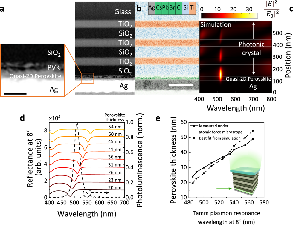
a Cross-sectional HAADF-STEM image of the perovskite-based Tamm plasmon structure. Left: Magnified image of the metal-quasi-2D perovskite interface. The scale bar shows 50 nm. A similar structure is fabricated as the reference-perovskite structure (without TiO2/SiO2 layer pairs) to ensure results are not affected by unwanted effects, e.g., PL quenching due to metal deposition. The thickness of each layer is TiO2 = (70 ± 2) nm, SiO2 = (90 ± 2) nm, quasi-2D perovskite + PVK = (34 ± 5) nm, Ag = (100 ± 5) nm.
b EDX chemical map of perovskite-based Tamm plasmon structure. Areas rich in Ag, Cs, Pb, Br, C, Si and Ti are marked in the legend. The scale bar shows 200 nm. The observed halo features at the titanium (Ti)-rich interface are found to be a slight compositional gradient of Ti, while the oxygen composition remains constant at the interface.
c Simulated electric field enhancement, |𝐸|2/|𝐸0|2 of the narrow-angle-Tamm-plasmon-perovskite structure.
d Experimental optimisation of perovskite-based Tamm-plasmon structure by varying the perovskite thicknesses between 20 nm to 54 nm (Tamm plasmon resonance wavelength best fitted with transfer matrix model to estimate thickness of perovskite). Tamm plasmon resonance dip acquired from reflectance measurements at 8°. PL of quasi-2D perovskite thin film on glass is shown as dashed line.
e Tamm plasmon resonance wavelength at 8° versus perovskite film thickness. Perovskite thickness is measured under AFM (solid line) and estimated from Tamm plasmon resonance wavelength best fitted with simulation (dashed line). Inset: schematic of the perovskite-based Tamm-plasmon structure with a green arrow indicating the quasi-2D perovskite layer.
Informację przesłali
Piotr NYGA, Michał NOWAK